This is the multi-page printable view of this section. Click here to print.
Reference
- 1: Benchmarks
- 2: Compiler
- 2.1: Structure diagram
- 2.2: Frontend
- 2.3: Opsets
- 2.4: Memory manager
- 2.5: High-level intermediate representation
- 2.6: Scheduler
- 2.7: Low-level intermediate representation
- 2.8: Backend
- 3: Hardware
- 3.1: Architectural paremeters
- 3.2: Architecture diagram
- 3.3: Configuration registers
- 3.4: Instruction set
- 3.5: Performance samples
1 - Benchmarks
Methodology
Benchmarks are generated using the Tensil compiler. Each instruction is evaluated against a latency model to compute expected execution time. Actual results may therefore differ somewhat from the numbers listed here. Help us improve the latency model!
ResNet-20v2
Trained for CIFAR.
| FPGA Board | Tensil Array Size | Clock (MHz) | Latency (ms) | Frames per second |
|---|---|---|---|---|
| Arty A7-35 | 8x8 | 150 | 21 | 48 |
| Pynq Z1 | 12x12 | 150 | 14 | 71 |
| Ultra96-V2 | 16x16 | 300 | 4 | 250 |
YoloV4-tiny
Trained for ImageNet.
| FPGA Board | Tensil Array Size | Clock (MHz) | Latency (ms) | Frames per second |
|---|---|---|---|---|
| Arty A7-35 | 8x8 | 150 | 175 | 5.7 |
| Pynq Z1 | 12x12 | 150 | 112 | 8.9 |
| Ultra96-V2 | 16x16 | 300 | 36 | 28 |
ResNet-50v2
Trained for ImageNet.
| FPGA Board | Tensil Array Size | Clock (MHz) | Latency (ms) | Frames per second |
|---|---|---|---|---|
| Arty A7-35 | 8x8 | 150 | 1969 | 0.5 |
| Pynq Z1 | 12x12 | 150 | 833 | 1.2 |
| Ultra96-V2 | 16x16 | 300 | 260 | 3.8 |
2 - Compiler
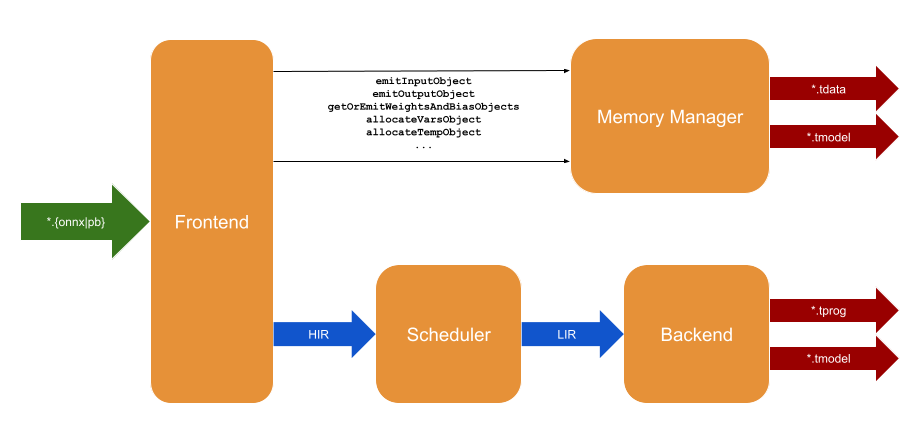
2.1 - Structure diagram
2.2 - Frontend
The frontend is responsible for handling the compiler’s primary input–an ML model. With many ML frameworks in existence, the compiler isolates the specific framework support in the frontend. In other words, we envision multiple dedicated frontends able to handle models created by each ML framework. Currently, there are two frontends supporting TensorFlow and ONNX with input in the form of model.pb and model.onnx files correspondingly. The frontend parses the model, represented in the form of a graph. It uses one or more output nodes to linearize the graph in a series of nodes respecting dataflow dependencies.
The frontend then processes this linearized series. During this processing, the frontend is grouping model nodes to form layers. Each layer represents one entire cycle started with matrix multiplication, followed by a series of accumulator operations and finalized with moving the result out of accumulators. In essence, the content of accumulators and systolic array weights is never shared between layers.
The frontend interacts with the memory manager to obtain necessary memory objects. There are two banks of memory directly accessible to the host: DRAM0 and DRAM1. The compiler dedicates DRAM0 to store variable data objects (Vars) such as inputs, outputs, and the data passed between layers. Next, it dedicates DRAM1 to various constants (Consts), such as matrix multiplication weights and bias, constants used in accumulator operations, and constants used to blend with variable data objects (like zero-padding). The frontend creates a new instance of the scheduler for each layer and submits a series of high-level intermediate representation (HIR) operations based on model nodes present in the layer. The frontend allocates special temporary (Temp) memory objects to pass the data between HIR operations within a single layer. The scheduler is later responsible for mapping this temporary memory to available accumulators.
2.3 - Opsets
Tensorflow
| Operation | Comments |
|---|---|
| MatMul | |
| Conv2D | Only SAME and VALID paddings are supported. |
| BiasAdd | |
| ResizeBilinear | Resize image with align corners is not supported. |
| FusedBatchNormV3 | |
| MaxPool | Only SAME and VALID paddings are supported. |
| AvgPool | Only SAME and VALID paddings are supported. |
| Mean | Only channel mean is supported. |
| Relu | |
| LeakyRelu | |
| AddV2 | |
| ConcatV2 | Only last dimension concat is supported. |
| Split | Only last dimension split is supported. |
| SplitV | Only last dimension split is supported. |
| Pad | Only 4D padding is supported. Only height/width padding is supported. |
| Reshape | |
| Cast* | Only DT_INT32 to DT_FLOAT cast is supported. |
| Tile* | |
| Pack* | Only first axis pack is supported. |
| StridedSlice* | Only 1D strided slice is supported. Only strided slice with shrink axis is supported. |
| Shape* |
- Only compile-time constants folding
Onnx
We support a subset of ONNX v8.
2.4 - Memory manager
The memory manager is responsible for allocating and freeing, when necessary, memory objects. Memory object represents a series of memory addresses (memory span) with associated tensor dimensions. The scheduler uses dimensions to ensure the correctness of the dataflow. In addition, the memory manager is tracking pending constants found in model nodes. The pending means that when the frontend processes the constant, it is unknown if it will become a memory object or be used as a parameter to one of the HIR operations. When a pending constant becomes a Const memory object, it gets emitted as a part of the model.tdata file later used by the driver to place into host memory. The memory manager also emits a memory map for Consts and Vars memories. Such a map is included in model.tmodel file to inform the driver of the memory layout to place the content of model.tdata file, as well as model’s inputs and outputs.
2.5 - High-level intermediate representation
High-level intermediate representation (HIR) is an interface offered by the scheduler. It expresses common ML operations abstract from specific ML frameworks, such as ONNX. It also operates in terms of memory objects.
Following are a few examples of HIR.
def emitMatMul(
      weightsObjs: Seq[MemoryObject],
      biasObj: Option[MemoryObject],
      inputOutputPairs: Seq[MemoryOptionalInputOutputObjects]
  ): Unit
The emitMatMul function takes weights and the bias memory objects, and a sequence of input-output object pairs. It performs matrix multiplication for each input memory object and places results in the output memory object. Input is optional, in which case it is assumed to be all zeroes. Weights and the bias must be Consts objects. Input must be Vars object, and output must be Temp object.
def emitRelu(
      inputObj: MemoryObject,
      outputObj: MemoryObject
  ): Unit
The emitRelu function performs ReLU activation on the input object and places the result in the output object. Both input and output must be Temp objects.
def emitSave(
      inputObj: MemoryObject,
      outputObj: MemoryObject
  ): Unit
The emitSave function moves data from the Temp input object to Vars output object, usually at the end of the layer.
2.6 - Scheduler
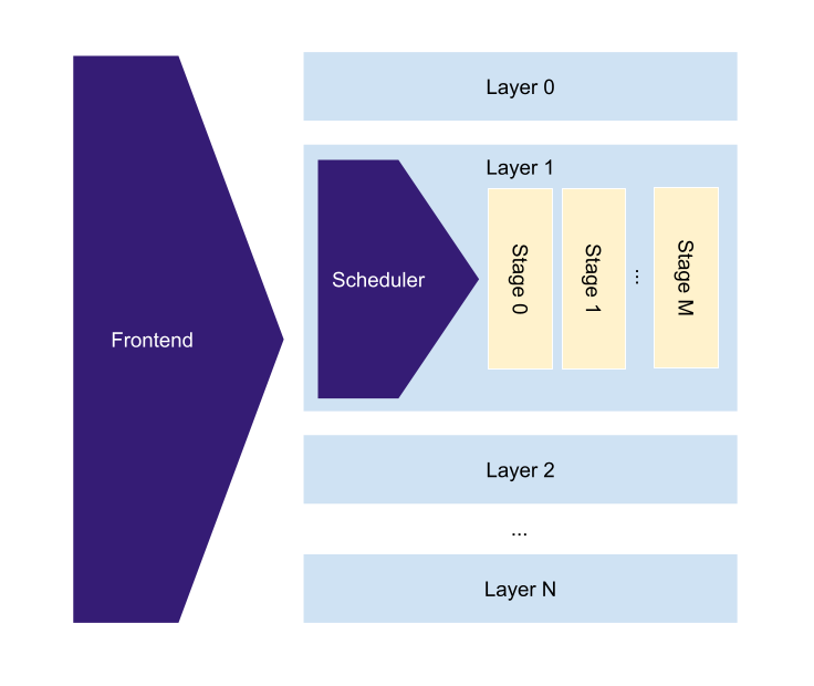
The scheduler is responsible for transforming the high-level intermediate representation (HIR) produced by the frontend to the low-level intermediate representation (LIR) consumed by the backend. The main objective of such transformation is to schedule HIR operations expressed in terms of relatively large Vars, Consts, and unlimited Temp memories to limited SRAM local memory and accumulators available to a specific configuration of the processing unit. Internally it achieves this by building a dataflow graph based on memory addresses and finding its maximum partitioning that fits the local memory and accumulators. Such a partition is called a stage. The scheduler then produces LIR for every stage independently. Like for the frontend layers, stages don’t share weights in the systolic array nor the content of accumulators. At the moment, they don’t share data in the local memory either, which we expect to change once the compiler has to work efficiently with larger-sized local memory.
2.7 - Low-level intermediate representation
Low-level intermediate representation (LIR) is an interface offered by the backend. It expresses instructions supported by the processing unit. Unlike HIR, it operates in terms of memory addresses. Each memory address is tagged with its memory type. While HIR memory objects are expected to contain Vars, Consts and Temp tagged addresses, LIR only accepts Vars, Consts, Local memory, and Accumulator tagged addresses. One of the key scheduler roles is to do this translation.
Following are a few examples of LIR. Each produces the corresponding processing unit instruction. Note that LIR is not using instruction flags directly. The backend role is to infer these flags based on LIR arguments, such as accumulate and toLocal booleans and memory address tags.
def emitMatMul(
      accumulate: Boolean,
      localStride: Int,
      localAddress: MemoryAddress,
      accumulatorStride: Int,
      accumulatorAddress: MemoryAddress,
      size: Long,
      comments: List[String] = List()
  ): Unit

def emitSIMD(
      accumulate: Boolean,
      simdOp: Int,
      simdSourceLeft: Int,
      simdSourceRight: Int,
      simdDestination: Int,
      writeAccumulatorAddress: MemoryAddress,
      readAccumulatorAddress: MemoryAddress,
      comments: List[String] = List()
  ): Unit

def emitDataMove(
      toLocal: Boolean,
      accumulate: Boolean,
      localAddress: MemoryAddress,
      address: MemoryAddress,
      size: Long,
      comments: List[String] = List()
  ): Unit
2.8 - Backend
The backend is responsible for translating LIR into the model.tprog and model.tmodel files containing the binary representation of the processing unit program and the information required by the driver to feed the program into the processing unit. It computes the instruction layout based on compiler options such as memory and SIMD registers depth. To produce instruction binary form, the backend infers instruction flags based on LIR arguments.
3 - Hardware
3.1 - Architectural paremeters
| Parameter | Description | Allowable values | Example value |
|---|---|---|---|
| Data type | The numerical format used to perform calculations in hardware | FP16BP8,FP32B16 |
FP16BP8, which means “Fixed point format with width 16 bits and with the binary point at 8 bits” |
| Array size | The size of the systolic array and also the number of scalars in each vector | 2-256 | 8 |
| DRAM0 depth | The number of vectors allocated in DRAM bank 0 | 2^{1-32} | 1048576 (= 2^20) |
| DRAM1 depth | The number of vectors allocated in DRAM bank 1 | 2^{1-32} | 1048576 (= 2^20) |
| Local depth | The number of vectors allocated in on-fabric main memory | 2^{1-16} | 16384 (= 2^14) |
| Accumulator depth | The number of vectors allocated in on-fabric accumulator memory | 2^{1-16} | 4096 (= 2^12) |
| SIMD registers depth | The number of registers to instantiate for each ALU in the SIMD module | 0-16 | 1 |
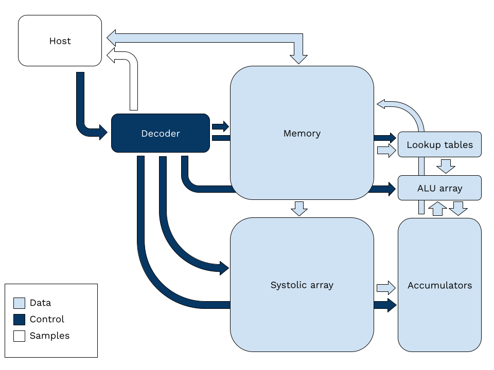
3.2 - Architecture diagram
3.3 - Configuration registers
| Name | Meaning | Width (bits) | Number | Default value |
|---|---|---|---|---|
| DRAM0 address offset* | The offset in DRAM of the memory space allocated for use by the DRAM0 interface | 32 | 0x00 | 0x0000 |
| DRAM0 cache behaviour | This register is passed without modification to the AXI converter for the DRAM0 interface, where it is used as the value of the AxCACHE field in both reads and writes. Default value of 0b0000 indicates no caching allowed. See AXI4 protocol spec for more details. | 4 | 0x01 | 0b0000 |
| <unused> | - | - | 0x02-0x03 | - |
| DRAM1 address offset* | The offset in DRAM of the memory space allocated for use by the DRAM1 interface | 32 | 0x04 | 0x0000 |
| DRAM1 cache behaviour | This register is passed without modification to the AXI converter for the DRAM1 interface, where it is used as the value of the AxCACHE field in both reads and writes. Default value of 0b0000 indicates no caching allowed. See AXI4 protocol spec for more details. | 4 | 0x05 | 0b0000 |
| <unused> | - | - | 0x06-0x07 | - |
| Timeout | The number of cycles the decoder will remain in the same state before raising the timeout flag. This usually indicates something has stalled and is useful for triggering debug ILAs. | 16 | 0x08 | 0x0064 |
| Tracepoint | The value of the program counter at which the tracepoint flag will be raised. Useful for triggering debug ILAs to inspect hardware state during execution. | 32 | 0x09 | 0xFFFFFFFF |
| Program counter | Increments by 1 every time an instruction is completely processed. | 32 | 0x0A | 0x00000000 |
| Sample interval | The period in cycles at which to sample the program counter and decoder control bus handshake signals. Default value of 0x0000 disables sampling. | 16 | 0x0B | 0x0000 |
*DRAM address offsets are specified in 64K blocks. The real address offset is 2^16 times the address offset register value configured. That is, if the DRAMx address offset register is configured with value 0x0001, the actual address offset that will appear in requests on the AXI bus will be 0x00010000.
3.4 - Instruction set
| Name | Description | Opcode | Flags | Operand #0 | Operand #1 | Operand #2 |
|---|---|---|---|---|---|---|
| NoOp | Do nothing | 0x0 | - | - | - | - |
| MatMul | Load input at memory address into systolic array and store result at accumulator address | 0x1 | Accumulate? Zeroes? | Local Memory stride/address | Accumulator stride/address | Size |
| DataMove | Move data between the main memory and either the accumulators or one of two off-chip DRAMs | 0x2 | Data flow control enum (see below) | Local Memory stride/address | Accumulator or DRAM stride/address | Size |
| LoadWeight | Load weight from memory address into systolic array | 0x3 | Zeroes? (Ignores operand #0) | Local Memory stride/address | Size | - |
| SIMD | Perform computations on data in the accumulator | 0x4 | Read? Write? Accumulate? | Accumulator write address | Accumulator read address | SIMD sub-instruction |
| LoadLUT | Load lookup tables from memory address. | 0x5 | - | Local Memory stride/address | Lookup table number | - |
| <unused> | - | 0x6-0xE | - | - | - | - |
| Configure | Set configuration registers | 0xF | - | Register number | Value | - |
Notes
-
Weights should be loaded in reverse order
-
Since Size = 0 doesn’t make sense, the size argument is interpreted as 1 less than the size of data movement requested i.e.
- size = 0 means transfer 1 vector
- size = 1 means transfer 2 vectors
- size = 255 means transfer 256 vectors etc.
-
Instruction width is a parameter supplied to the RTL generator
- Opcode field is always 4 bits
- Flags field is always 4 bits
- Instruction must be large enough to fit the maximum values of all operands in the longest instruction (MatMul, DataMove, SIMD)
-
Flags are represented in the following order: [3 2 1 0]
- i.e. the first flag listed is at bit 0 (the 4th bit), second flag is at bit 1 (the 3rd bit) etc.
-
Arguments are in the following order: [2 1 0]
-
e.g. in MatMul the bits of the instruction will be, from most significant bit to least: opcode, optional zero padding, accumulate?, size, accumulator stride/address, memory stride/address
-
Address unit for all memories is one array vector
-
Stride has a fixed number of bits followed by the number of bits for the address of the largest memory that may appear in the operand. The address for smaller memories gets padded by zeros. Stride is encoded as power of 2. For example the 3-bit stride is as follows 000=1, 001=2, 010=4, 011=8,.. 111=128
-
e.g. in a 2-byte argument with an 11-bit address and a 3-bit stride, the bit layout would be
- 15:14 = padding, to be set to zeroes
- 13:11 = stride
- 10:0 = address
-
-
Size unit is one array vector
-
-
Data flow control enum flag values are:
- 0b0000 = 0 = 0x0 = DRAM0 to memory
- 0b0001 = 1 = 0x1 = memory to DRAM0
- 0b0010 = 2 = 0x2 = DRAM1 to memory
- 0b0011 = 3 = 0x3 = memory to DRAM1
- …
- 0b1100 = 12 = 0xc = accumulator to memory
- 0b1101 = 13 = 0xd = memory to accumulator
- 0b1110 = 14 = 0xe = <reserved>
- 0b1111 = 15 = 0xf = memory to accumulator (accumulate)
-
SIMD instructions have some subtleties
-
can read or write (+accumulate) in the same instruction
-
when the read flag is set, data is read from the accumulators into the ALU array
-
when the write flag is set, the ALU array output is written into the accumulators
-
the accumulate flag determines whether this is an accumulate or an overwrite
-
the output to be written is computed from the input that was read in on the same instruction
- i.e. if `x` is read from the accumulators at the specified read address, and the ALU computes `f(_)` then `f(x)` will be written to the accumulators at the specified write address from the same instruction
-
data is output from the ALU array on every instruction i.e. even if the destination is specified as register 1, you can still write into the accumulators from the output
-
-
before reading out from the accumulators with a DataMove, you should wait at least 2 instructions since the last SIMD instruction in which the write flag was high. This is because the data takes about 2 instructions to propagate into the accumulators from the ALUs. The easiest way to achieve this is just to insert 2 no-ops before the DataMove instruction.
- 2 instructions is an empirical estimate. The number may need to be higher in certain cases. If you see data being dropped/corrupted/repeated, talk to[email protected] about it
-
SIMD sub-instructions
All SIMD instructions are composed of 4 parts: opcode, source left, source right and destination. The widths are as follows:
-
opcode = ceil(log2(numOps))
- numOps is currently fixed at 16, so opcode is 4 bits
-
source left = ceil(log2(numRegisters+1))
- numRegisters is currently fixed at 1, so source left is 1 bit
-
source right = source left
-
dest = source left
Source left is the left argument for binary operations, and the single argument for unary operations. Source right is the right argument for binary operations, and is ignored for unary operations.
The_Move_ opcode allows you to move data from one register to another, or to read the data in a register to output. The _NoOp_ opcode is only a true no-op when both the read and write flags are set to false in the SIMD instruction. Otherwise, _NoOp_ has an overloaded meaning: it is used to trigger an external read or write. That is, to write into the accumulators from the PE array, or to read out from the accumulators into on-chip main memory.
| Opcode | Source left | Source right | Destination |
|---|---|---|---|
| 0x00 = NoOp** 0x01 = Zero 0x02 = Move* 0x03 = Not* 0x04 = And 0x05 = Or 0x06 = Increment* 0x07 = Decrement* 0x08 = Add 0x09 = Subtract 0x0A = Multiply 0x0B = Abs* 0x0C = GreaterThan 0x0D = GreaterThanEqual 0x0E = Min 0x0F = Max 0x10 = Lookup* |
0 = input 1 = register 1 2 = register 2… |
0 = input 1 = register 1 2 = register 2… |
0 = output 1 = output & register 1 2 = output & register 2… |
*unary operation
**arguments are ignored
Lookup sub-instruction
The lookup sub-instruction returns_N+1_ result values where _N_ is the number of lookup tables in the architecture. The results are, in order
- the difference between the argument and the closest key found in the lookup table index
- the value found in the first lookup table
- the value found in the second lookup table
- etc.
The destination register_d_specifies the register which will receive the first result i.e. the difference. The remaining results will be populated in the registers numbered ascending from_d_, so that the result from lookup table_i_ will be written to register _d+i+1_. This assumes that the architecture is configured with sufficient registers to store all the results, and that_d+N_ <= total number of registers. The behaviour of the lookup sub-instruction is undefined if these requirements aren’t met.
3.5 - Performance samples
Performance sampling
The program counter and decoder control bus handshake signals can be sampled at a fixed interval of L cycles in order to measure system performance. The samples are written out to the sample IO bus in blocks of N sample words. The block is terminated by asserting the AXI stream TLAST signal. Each sample word is a 64-bit word, with the following meaning:
| Bus name | Signal | Bit field(s) | Comments |
|---|---|---|---|
| Program counter | 0:31 | Contains all 1s if the sample is invalid. Invalid samples are produced when the sampling interval is set to 0. | |
| Array | Valid | 32 | Contains all 0s if the sample is invalid. |
| Ready | 33 | ||
| Acc | Valid | 34 | |
| Ready | 35 | ||
| Dataflow | Valid | 36 | |
| Ready | 37 | ||
| DRAM1 | Valid | 38 | |
| Ready | 39 | ||
| DRAM0 | Valid | 40 | |
| Ready | 41 | ||
| MemPortB | Valid | 42 | |
| Ready | 43 | ||
| MemPortA | Valid | 44 | |
| Ready | 45 | ||
| Instruction | Valid | 46 | |
| Ready | 47 | ||
| <unused> | 48:64 |
Value of L can be changed by setting the configuration register. Value of N is defined by architecture.