Integrate the Tensil RTL
Things you’ll need
- an FPGA board (e.g. the Ultra96-V2)
- an EDA tool that can target your FPGA (e.g. if you purchased an Ultra96-V2, it should have come with a free license to Xilinx Vivado)
- the set of RTL (
*.v) files that were emitted by the RTL generator. If you don’t have those, see how to generate RTL
This guide will assume you are using the Xilinx Vivado block design interface, but the methodology should be broadly the same for any EDA tool.
1. Instantiate the IP block
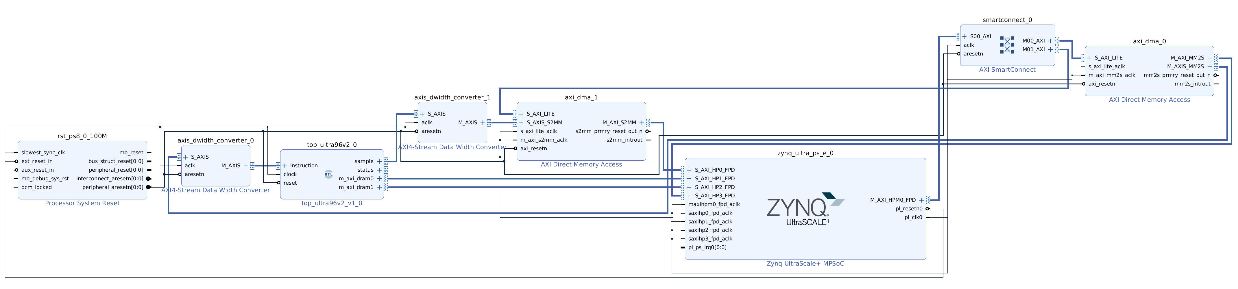
Create a new project, choose the appropriate board constraints file and add a block design. Instantiate the host processor: in the case of the Ultra96-V2, this will be the Zynq UltraScale+ processing system. Be sure to run any block automation required.
Move the generated RTL files into your project sources. In Vivado this can be achieved by hitting Add sources and selecting the files. Make sure to add all generated files. If you generated them using the guide, the files will be called top_ultra96v2.v, bram_dp_256x20480.v and bram_dp_256x4096.v.
Then, drag and drop the Top block (named top_<arch>.v, e.g. top_ultra96v2.v) into the block design. We’ll refer to this block as the top block from here on.
2. Connect the AXI interfaces
There are three AXI interfaces needed for basic operation, one for receiving instructions and two for interacting with host memory.
The instruction interface is an AXI stream slave that needs to be driven by the host processor. The easiest way to achieve this is to instantiate an AXI DMA block with one write port. Connect the AXI stream master (M_AXIS_MM2S) to the instruction interface on the top block. You may need to use an AXI data width converter to ensure the widths match.
Next, connect the memory interfaces. The host processor should have AXI slave ports that provide access to host memory, although these may need to be enabled in the configuration settings. For Ultra96-V2, go to the PL Interfaces section and enable S_AXI_HP0_FPD and S_AXI_HP2_FPD. On the top block, connect m_axi_dram0 -> S_AXI_HP0_FPD and connect m_axi_dram1 -> S_AXI_HP2_FPD.
3. Generate bitstream
The block design should now be complete. See below for an example of what a complete design looks like (you can ignore the sample and status interfaces: they are for performance testing and debugging respectively).
Save your design and then create a HDL wrapper if necessary. Finally, start the implementation by hitting “Generate bitstream”. This may take around 10 minutes. If all goes well, you should end up with a .bit file, which is the bitstream itself, and possibly a hardware hand-off file with an extension like .hwh. For Vivado, bitstream can be found at <project_name>.runs/impl_1/design_1_wrapper.bit and the hardware handoff file can be found at <project_name>.srcs/sources_1/bd/design_1/hw_handoff/design_1.hwh.
Next Steps
Now that you have a hardware implementation, you are ready to run your compiled ML model.
Troubleshooting
How to integrate the RTL block will vary from system to system, and there are many quirks and gotchas that could get in the way. If you get stuck, don’t despair! We’re here to help: ask a question on Discord or email us at [email protected].