Getting Tensil to run ResNet at 300 frames per second on ZCU104
Originally posted here.
Introduction
Sometimes the application requires pushing the performance to its limits. In this tutorial we will show how to optimize Tensil running ResNet20 trained on CIFAR for maximum performance. To do this, we will use the powerful ZCU104 board and implement an embedded application to remove the overhead of running Linux OS and PYNQ. Importantly, we still won’t quantize the model and use Tensil with 16-bit fixed point data type. We will demonstrate that running the CIFAR test data set shows very little accuracy drop when rounding down from the original 32-bit floating point.
We will be using Vivado 2021.1, which you can download and use for free for educational projects. Make sure to install Vitis, which will include Vivado and Vitis. We will use Vitis for building the embedded application.
Tensil tools are packaged in the form of Docker container, so you’ll need to have Docker installed and then pull Tensil Docker image by running the following command.
docker pull tensilai/tensil
Next, use docker run command to launch Tensil container.
docker run \
    -u $(id -u ${USER}):$(id -g ${USER}) \
    -v $(pwd):/work \
    -w /work \
    -it tensilai/tensil \
    bash
You will also need to clone the tutorial GitHub repository. It contains necessary source files as well as all of the intermediate artifacts in case you would like to skip running Tensil tools or Vivado.
Baseline solution
We start with the baseline solution, in which we will create a working Tensil application with default design choices. Once we have a stable working solution we will look at opportunities to improve its performance.
Tensil RTL and Vivado implementation
Let’s start with generating Tensil RTL. Run the following command to generate Verilog artifacts.
tensil rtl -a /demo/arch/zcu104.tarch -d 128 -s true -t vivado/baseline
You can skip running the Tensil RTL tool and grab the baseline Verilog artifacts here.
Note that we need to specify the data width for AXI interfaces to be 128 bits, so that they fit directly with AXI ports on the ZYNQ UltraScale+ device at the heart of the ZCU104 board.
Next, create the new Vivado RTL project, select the ZCU104 board and import the three Verilog files produced by the Tensil RTL command.
We provide scripted block design, so that you won’t need to connect blocks manually. You can use Tools -> Run Tcl Script to run it. Once you have the design ready, right-click on tensil_zcu104 in the Design Sources pane and select Create HDL Wrapper. Let Vivado manage the wrapper. Once the wrapper is ready, right-click on tensil_zcu104_wrapper in the same Design Sources pane and select Set as Top.
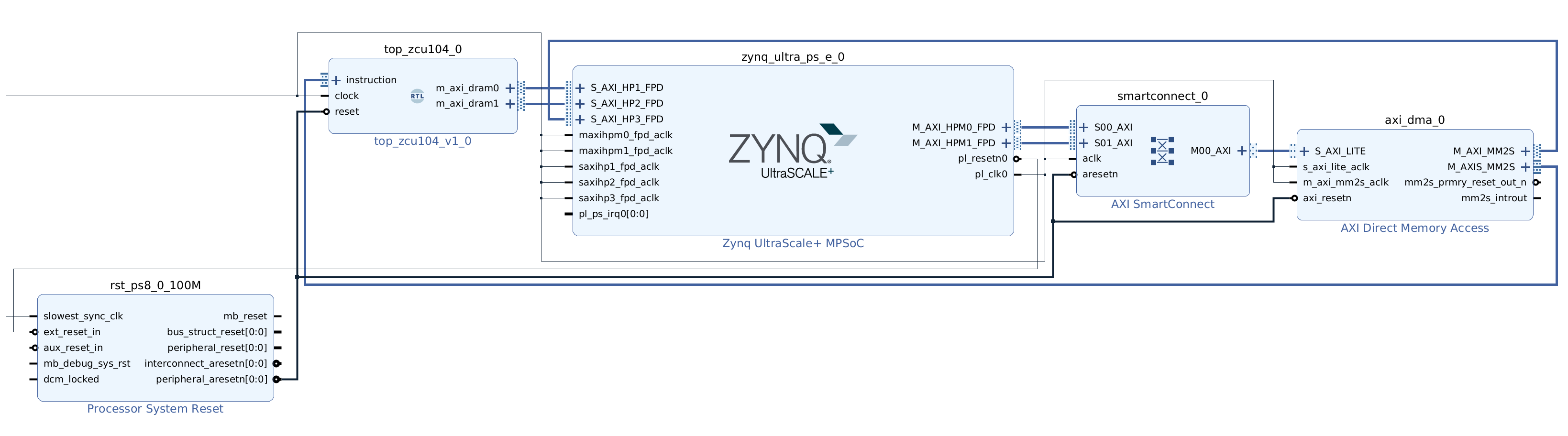
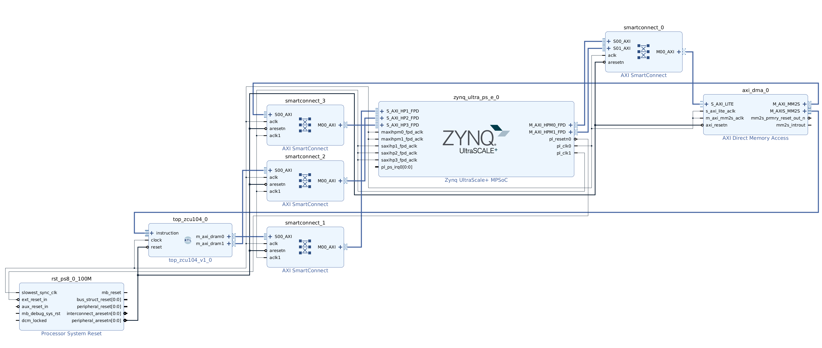
Following is how the baseline block design looks like. Note the direct connections between Tensil block AXI masters and ZYNQ AXI slaves. The instruction AXI stream port is connected via AXI DMA block.
Next, click on Generate Bitstream in the Flow Navigator pane. Once bitstream is ready click on File -> Export -> Export Hardware. Make sure that Include bitstream choice is selected. Now you have the XSA file containing everything necessary for Vitis to create the embedded application project.
You can skip the Vivado implementation and grab the baseline XSA file here.
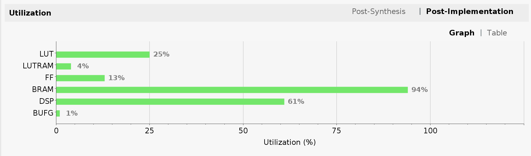
Another important result of running Vivado implementation is FPGA utilization. It is shown as one of the panes in the project summary once implementation is completed. The utilization is a direct function of our choice of Tensil architecture.
{
    "data_type": "FP16BP8",
    "array_size": 32,
    "dram0_depth": 2097152,
    "dram1_depth": 2097152,
    "local_depth": 16384,
    "accumulator_depth": 4096,
    "simd_registers_depth": 1,
    "stride0_depth": 8,
    "stride1_depth": 8,
    "number_of_threads": 1,
    "thread_queue_depth": 8
}
Specifying 32 by 32 systolic array size contributed to the high utilization of multiply-accumulate units (DSP). Note how we pushed Block RAM (BRAM) utilization almost to its limit by specifying 16 KV local memory and 4 KV accumulators (KV = 1024 vectors = 1024 * 32 * 16 bits).
ResNet compiled for Tensil
The ZCU104 board supports an SD card interface. This allows us to use Tensil embedded driver file system functionality to read the ResNet model and a set of images to test it with. The set we will be using is the test set for the original CIFAR-10. The ResNet model is trained with the separate training and validation sets from the CIFAR-10. The test set is what the model hasn’t seen in training and therefore gives an objective estimate of its accuracy. The CIFAR-10 provides the test set of 10,000 images in several formats. We will use the binary format that is more suitable for the embedded application.
Let’s start with compiling the ResNet ONNX file to Tensil model artifacts. The following command will produce *.tmodel, *.tdata and *.tprog files under the sdcard/baseline/ directory. The *.tmodel file is a JSON-formatted description of the Tensil model, which references *.tdata (model weights) and *.tprog (model program for the Tensil processor.)
tensil compile \
    -a /demo/arch/zcu104.tarch \
    -m /demo/models/resnet20v2_cifar.onnx \
    -o "Identity:0" \
    -s true \
    -t sdcard/baseline/
Once compiled, copy the content of the sdcard directory, which should also include the CIFAR-10 test data set (test_batch.bin) to the FAT-formatted SD card. Insert the card into the ZCU104 SD card slot.
You can skip the model compilation step and use the sdcard directory in our GitHub repository.
Tensil for Vitis embedded applications
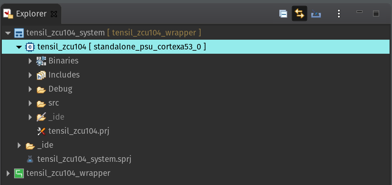
Launch Vitis IDE and create a new workspace for our project. Once greeted by the welcome screen click on Create Application Project. On the subsequent screen select Create a new platform from hardware (XSA) and select the XSA file produced in the previous section. Name the application project tensil_zcu104. Keep default choices in the next few screens. On the last screen select Empty Application (C).
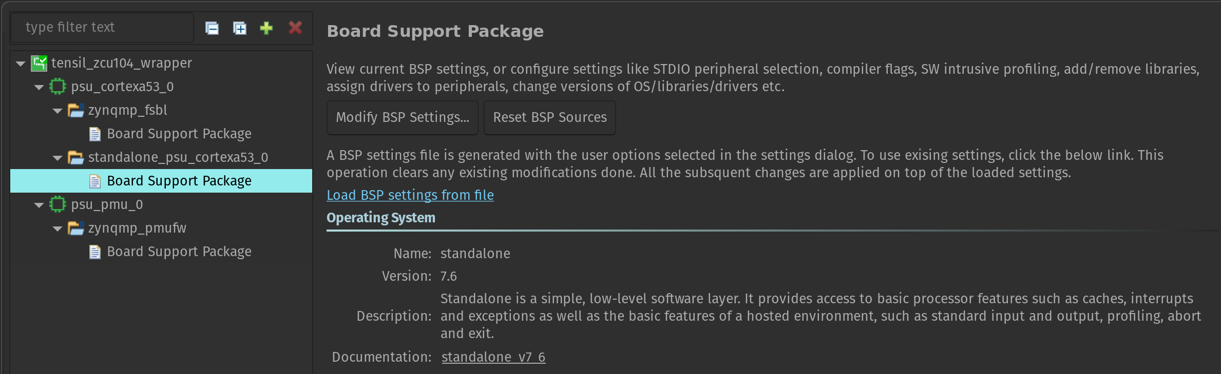
Now let’s make one important adjustment to the platform. Right-click on the tensil_zcu104 [Application] project in the Assistant pane and select Navigate to BSP settings. You will see a tree containing psu_cortex53_0 (the ARM cores we will be running on) with zynqmp_fsbl (first stage bootloader) and standalone_psu_cortex53_0 (our application) subnodes. Board Support Package under standalone should be selected.
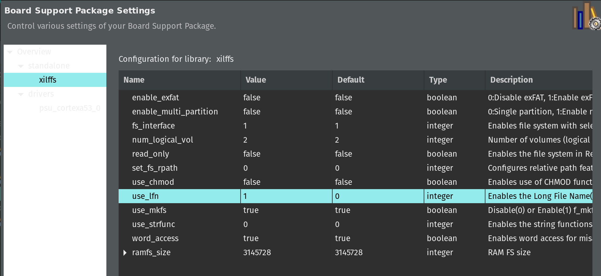
In the Board Support Package pane click on Modify BSP settings. In Overview click the checkbox for xilff. This will enable the FAT filesystem driver for the SD card slot supported by the ZCU104 board. Click on xilff that should have appeared under Overview in the left-side pane. Change use_lfn from 0 to 1. This will enable long file name support for the FAT filesystem driver.
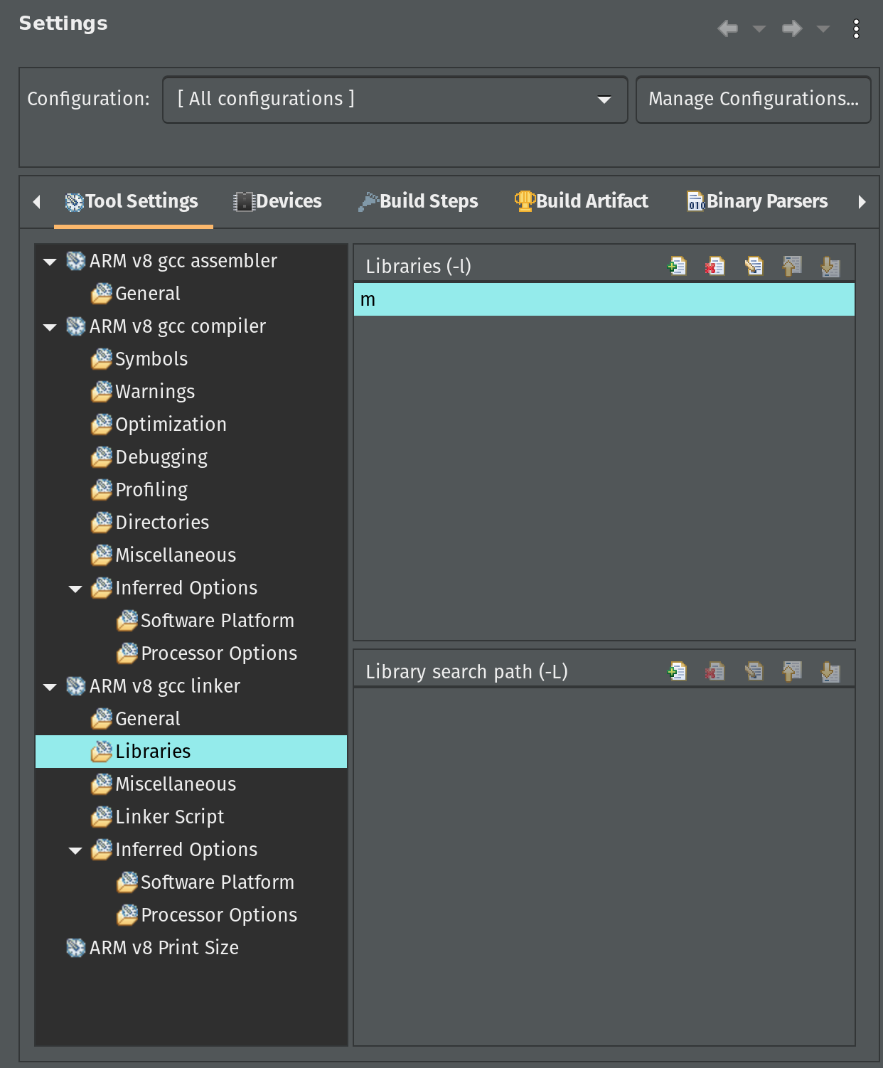
Before we copy all necessary source files, let’s adjust application C/C++ build settings to link our application with the standard math library. In the Explorer pane right-click the tensil_zcu104 application project. Select C/C++ Build Settings from the menu.
Click on Configuration dropdown and choose All configurations. Then, under ARM v8 gcc linker click on Libraries. In the Libraries pane click on the add button and enter m.
Now, let’s copy all necessary source files. For this you will need to clone the tutorial GitHub repository as well as the Tensil GitHub repository for the embedded driver sources. But first, let’s copy architecture parameters for the embedded driver from the output artifacts of Tensil RTL tool.
cp \
    <tutorial repository root>/vivado/baseline/architecture_params.h \
    <Vitis workspace root>/tensil_zcu104/src/
Next, copy the embedded driver.
cp -r \
    <Tensil repository root>/drivers/embedded/tensil \
    <Vitis workspace root>/tensil_zcu104/src/
Lastly, copy the ZCU104 embedded application. Note that platform.h copied in the previous step gets overwritten.
cp -r \
    <tutorial repository root>/vitis/* \
    <Vitis workspace root>/tensil_zcu104/src/
Finally, let’s build and run the application. First, make sure the ZCU104 board has boot DIP switches (SW6) all in ON position (towards the center of the board) to enable booting from JTAG. Then, right-click on the Debug entry under the tensil_zcu104 [Application] project in the Assistant pane and select Debug -> Launch Hardware.
Start the serial IO tool of your choice (like tio) and connect to /dev/ttyUSB1 at 115200 baud. It could be a different device depending on what else is plugged into your computer. Look for a device name starting with Future Technology Devices International.
tio -b 115200 /dev/ttyUSB1
With the SD card inserted and containing the CIFAR-10 test data set and the ResNet model compiled for Tensil you should see the inference printing every 100’s image and the corresponding prediction along with measured inferences (frames) per second.
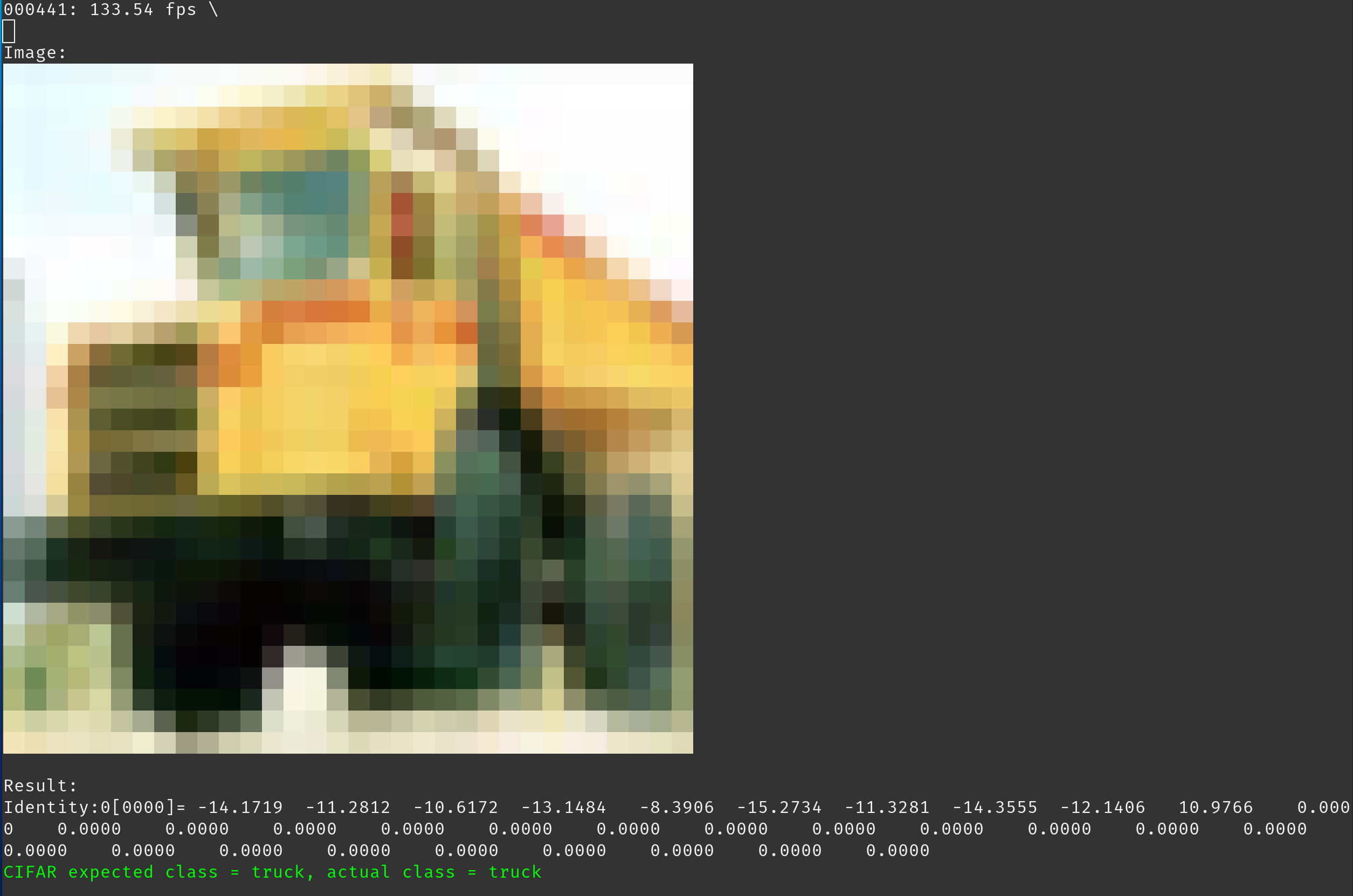
After running the inference on the entire test data set the program will print the final average frames per second and the accuracy of the inference. For the baseline solution we are getting an average of 133.54 frames per second with 90% accuracy. Note that the accuracy we are seeing when testing the same ResNet model with TensorFlow is 92%. The 2% drop is due to changing the data type from 32-bit floating point in TensorFlow to 16-bit fixed point in Tensil.
Dual clock solution
The first optimization is based on the following observation. The Tensil RTL block is clocked at 100MHz. (We could clock it higher, but for the purpose of this tutorial let’s assume this is our maximum clock.) The Tensil block DRAM0 and DRAM1 ports are connected to AXI interfaces on the ZYNQ block. The instruction port is indirectly connected to the AXI on the ZYNQ block via AXI DMA. ZYNQ UltraScal+ AXI ports support up to 333MHz and the maximum width of 128 bits. This gives us the opportunity to introduce a second clock domain for 333MHz while at the same time making the Tensil AXI ports wider.
The following diagram shows how this may work in a simpler 100MHz to 400MHz, 512- to 128-bit conversion. Each clock in the Tensil clock domain would pump one 512-bit word in or out. This would match 4 clocks in the ZYNQ clock domain with 512-bit word split to or composed from 4 128-bit words.

First let’s use the -d argument in Tensil RTL command to generate the RTL with 512-bit interfaces.
tensil rtl -a /demo/arch/zcu104.tarch -d 512 -s true -t vivado/dual_clock
The AXI SmartConnect block allows for both AXI width adjustment and separate clock domains. We change our block design by inserting these blocks in all three connections between Tensil RTL and the ZYNQ AXI ports. We suggest following the steps above to create a new Vivado project for the dual clock design. Again, we provide scripted block design, so that you won’t need to connect blocks manually. Following is how the dual clock block design looks like.
You can skip the Vivado implementation and grab the dual clock XSA file here.
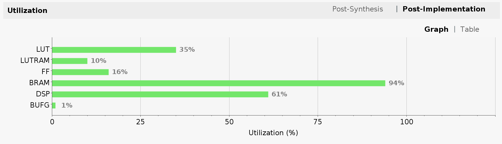
Let’s take a look at FPGA utilization for dual clock design. Note that the utilization for LUT, LUTRAM and FF has increased due to added AXI SmartConnect blocks and wider Tensil intefaces. BRAM and DSP utilization stayed the same since we did not change the Tensil architecture.
Now, we suggest you also create a new Vitis workspace for the dual clock design and follow the steps above to get the inference running. The model remains unchanged since we did not change the Tensil architecture.
For the dual clock solution we are getting an average of 152.04 frames per second–a meaningful improvement over the baseline. This improvement is roughly proportional to the ratio of time spent in moving data to and from the FPGA to the time spent in internal data movement and computation.
Ultra RAM solution
The second optimization is based on the higher-end ZYNQ UltraScale+ devices support for another type of on-chip memory called Ultra RAM. By default, Vivado maps dual-port memory to Block RAM. In order for it to map to the Ultra RAM it needs hints in the Verilog code. To enable these hints we will use --use-xilinx-ultra-ram option of the Tensil RTL tool. The amount of Ultra RAM available on ZCU104 allows us to add around 48 KV memory in addition to 20 KV available through Block RAM.
We start by creating a new Tensil architecture for ZCU104 in which we allocate all of the Block RAM (20 KV) to accumulators and all of the Ultra RAM (48 KV) to local memory.
{
    "data_type": "FP16BP8",
    "array_size": 32,
    "dram0_depth": 2097152,
    "dram1_depth": 2097152,
    "local_depth": 49152,
    "accumulator_depth": 20480,
    "simd_registers_depth": 1,
    "stride0_depth": 8,
    "stride1_depth": 8,
    "number_of_threads": 1,
    "thread_queue_depth": 8
}
Run the following command to generate Verilog artifacts.
tensil rtl \
    -a /demo/arch/zcu104_uram.tarch \
    -d 512 \
    --use-xilinx-ultra-ram true \
    -s true \
    -t vivado/ultra_ram
You can also skip running the Tensil RTL tool and grab the Ultra RAM Verilog artifacts here.
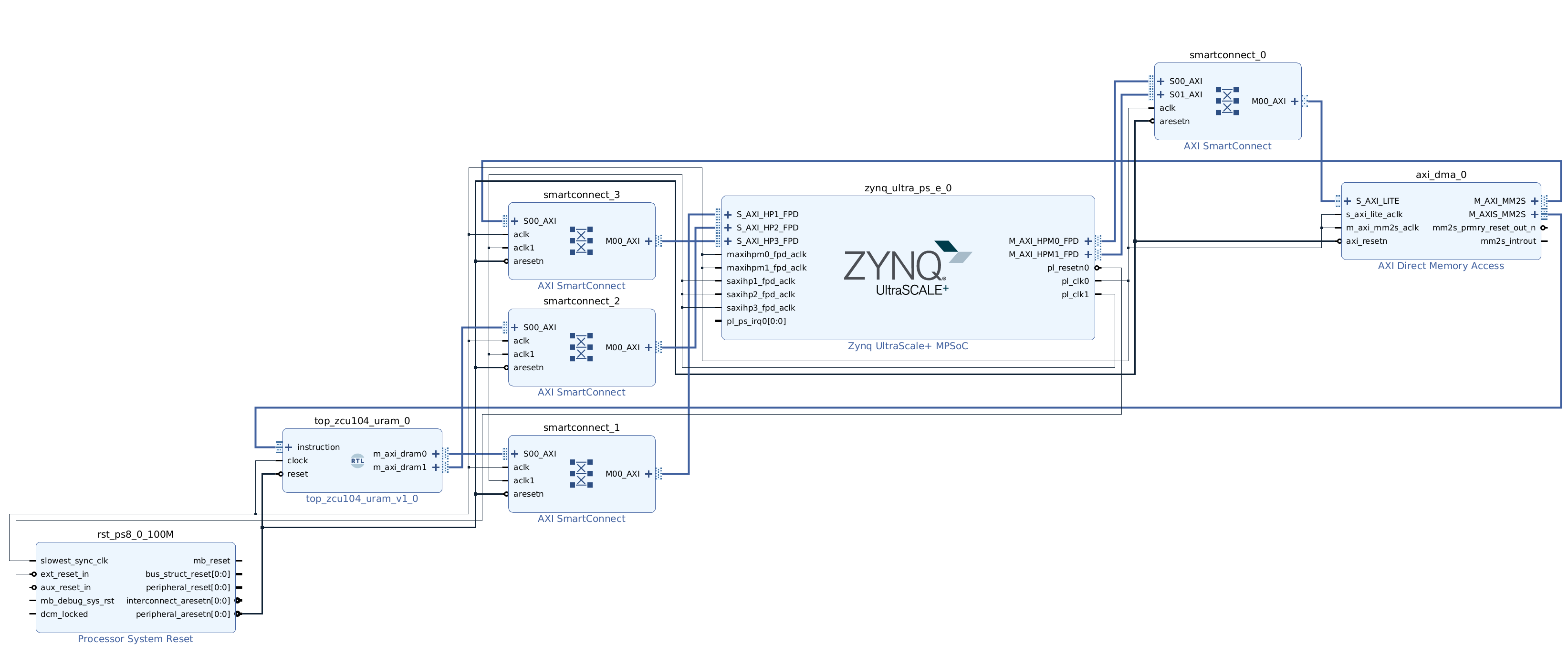
Follow the steps above to create a new Vivado project for Ultra RAM solution. We provide scripted block design, so that you won’t need to connect blocks manually. Following is how the Ultra RAM block design looks like. Note, that we based it on the dual clock design and the only difference is in the Tensil RTL block.
You can skip the Vivado implementation and grab the Ultra RAM XSA file here.
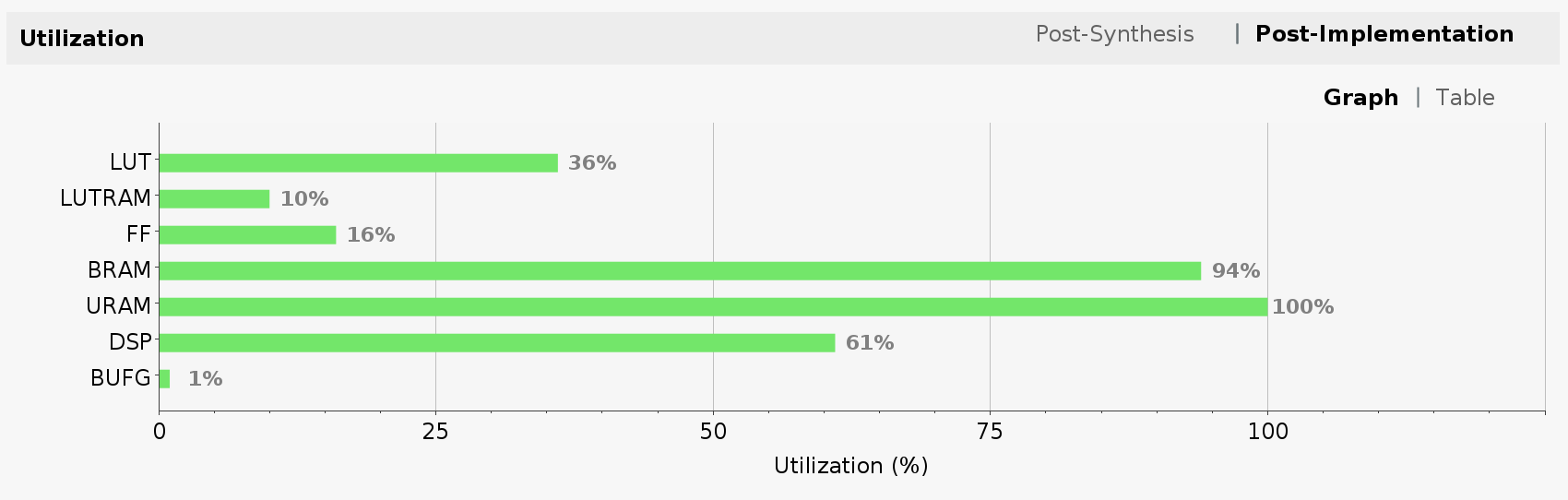
Now, let’s take a look at FPGA utilization for Ultra RAM design. Note that the utilization is mostly unchanged from the one of the dual clock design. The exception is the new line item for Ultra RAM (URAM), which we pushed to its full limit.
Because we changed the Tensil architecture the new model needs to be compiled and copied to the SD card.
tensil compile \
    -a /demo/arch/zcu104_uram.tarch \
    -m /demo/models/resnet20v2_cifar.onnx \
    -o "Identity:0" \
    -s true \
    -t sdcard/ultra_ram/
You can skip the model compilation step and use the sdcard directory in our GitHub repository.
We again, suggest you create a new Vitis workspace for the Ultra RAM design and follow the steps above to get the inference running. Make sure to uncomment the correct MODEL_FILE_PATH definition for the newly created *.tmodel file.
For the Ultra RAM solution we are getting an average of 170.16 frames per second, another meaningful improvement. This improvement is based purely on having larger on-chip memory. With a small on-chip memory the Tensil compiler is forced to partition ResNet convolution layers into multiple load-compute-save blocks. This, in turn, requires that the same input activations are loaded multiple times, assuming weights are loaded only once. This is called weight-stationary dataflow. In the future, we will add an option for input-stationary dataflow. With it, when partitioned, the input activations are loaded once and the same weights are loaded multiple times.
The following diagram shows such partitioned compilation. Layer N has 2 stages. In each stage a unique subset of weights is loaded. Then, each stage is further split into 2 partitions. Partition is defined by the largest amount of weights, input and output activations, and intermediate results that fit local memory and accumulators.

Having larger on-chip memory reduces this partitioning and, by extension, the need to load the same data multiple times. The following diagram shows how layer N now has 1 stage and 1 partition that fits larger local memory and accumulators, which allows weights and activations to be loaded only once.

Solutions with large local memory
The final optimization is based on the same hardware design and Tensil architecture we created to support the Ultra RAM. We will only change the Tensil compiler strategy.
As we mentioned previously, the Tensil compiler, by default, assumes that model is much larger in terms of its weights and activations than the local memory available on the FPGA. This is true for large models and for low-end FPGA devices. For small and medium sized models running on large FPGA devices there is a possibility that local memory is large enough to contain the weights plus input and output activations for each layer.
To see if this strategy is worth trying, we first look at the output of Tensil compiler for the ZCU104 architecture with the Ultra RAM.

The maximum number for stages and partitions being both 1 inform us that none of the layers were partitioned, or, in other words, each layer’s weights and activations did fit in the local memory. Another way to guide this decision is to use the --layers-summary true option with the Tensil compiler, which will report the summary per each layer with local and accumulator utilization.

Thus, the first strategy will be to try keeping activations in local memory between layers by specifying --strategy local-vars. The following diagram shows this strategy.

Run the following command and then copy the newly created model to the SD card.
tensil compile \
    -a /demo/arch/zcu104_uram.tarch \
    -m /demo/models/resnet20v2_cifar.onnx \
    -o "Identity:0" \
    -s true \
    --strategy local-vars \
    -t sdcard/ultra_ram_local_vars/
You can skip all of the model compilation steps in this section and use the sdcard directory in our GitHub repository.
This time, you can reuse the Vitis workspace for the Ultra RAM solution and simply uncomment the correct MODEL_FILE_PATH definition for each newly created *.tmodel file.
With the local-vars strategy we are getting an average of 214.66 frames per second.
Now that we have seen the improvement allowed by large on-chip memory, let’s see if any other load and save operations can be avoided. With local-vars strategy we load the input image and the weights and then save the output predictions. What if there would be enough on-chip memory to keep the weights loaded? There is a strategy for this!
With the local-consts strategy the inference expects all of the model weights to be preloaded to the local memory before the inference. This is the job for the driver. When the Tensil driver loads the model compiled with local-consts strategy it preloads its weights from *.tdata file into the local memory. The following diagram shows this strategy.

tensil compile \
    -a /demo/arch/zcu104_uram.tarch \
    -m /demo/models/resnet20v2_cifar.onnx \
    -o "Identity:0" \
    -s true \
    --strategy local-consts \
    -t sdcard/ultra_ram_local_consts/
With the local-consts strategy we are getting an average of 231.57 frames per second.
Finally, the local-vars-and-consts strategy combines local-vars and local-consts. With this strategy the inference will only load the input image and save the output predictions. The following diagram shows this strategy.

tensil compile \
    -a /demo/arch/zcu104_uram.tarch \
    -m /demo/models/resnet20v2_cifar.onnx \
    -o "Identity:0" \
    -s true \
    --strategy local-vars-and-consts \
    -t sdcard/ultra_ram_local_vars_and_consts/
With the local-vars-and-consts strategy we are getting an average of 293.58 frames per second.
Conclusion
In this tutorial we demonstrated how improving the Vivado hardware design, leveraging Xilinx Ultra RAM, and using the advanced compiler strategies can improve the performance of inference.
The following chart summarizes presented solutions and their frames per second performance.
